Article
Network On Chip
How FPGAs with NoCs can improve performance and productivity
Introduction
FPGA devices have become increasingly complicated, supporting numerous external interfaces such as memory and network connections. The IP and the communication logic for the numerous interfaces required can absorb a significant number of the reconfigurable resources on the FPGA, hence reducing logic available for compute. The vast number of routing resources required for interconnecting many high-speed connections can also cause bottlenecks in FPGA designs, resulting in a lower operating frequency and therefore lower performance. This is particularly true if there is a need for inter-communication between these interfaces.
Networks On Chips (NoCs) attempt to address this problem by providing dedicated routing and switching logic to make all interfaces visible to each other. This replaces user defined logic using FPGA gates, with a flexible generic hard-wired network.
A NoC provides a number of endpoints that are accessible to user gates, providing addressable access to any interface attached to the NoC, as well as user components that are also attached to a different endpoint.
Figure 1 illustrates a basic NoC with multiple user endpoints providing access to couple of NoC attached memories. NoCs are not like crossbars, which typically provide equal throughput regardless of how the endpoints are connected together. That means NoCs are vulnerable to congestion with certain access patterns. Figure 2 is an example of how congestion can occur. Some NoCs attempt to avoid such problems by running the network fabric at a much higher frequency than the FPGA logic or by providing multiple routes in high traffic regions.o

Figure 1 : Example NoC with memory endpoints
Figure 2 : Routing logic must be shared in NoCs when multiple endpoints are trying to access overlapping interfaces.
Advantages of FPGAs with NoCs
Some benefits of using a NoC are:
- A NoC removes the need to design custom arbitration logic for designs requiring shared access to multiple memory or Ethernet interfaces. An AFU endpoint can see all other attached AFU’s and memories, making all-to-all communications easier to implement.
- By removing inter-memory communications from the general FPGA routing logic, the FPGA place and route tools find placement far easier through better separation of resources. This increases the likelihood of achieving the target clock frequency.
- Some NoCs facilitate direct access from the host to device memories via the PCIe interface, again saving FPGA fabric for application work.
- External memory arbitration logic is provided via multiple NoC interfaces, with Quality of Service (QoS) built into the NoC. Multiple AFUs can share the same resource without requiring custom IP to do so.
There are some added design challenges to using a NOC:
- NoCs are high-speed networks and therefore can require relatively high amounts of power compared to general FPGA logic. This needs to be balanced against the power saving from using fewer FPGA resources. Power consumption can be reduced by lowering the NoC operating frequency and turning off unused elements of the NoC.
- The switching logic within a NoC will add latency to external communications. If an application is latency sensitive, using a NoC should be avoided. Some direct connections are typically provided to bypass the NoC in this scenario.
FPGA Devices with NoCs
Achronix 2D NoC
The Achronix Speedster7t devices use a 2D NOC that provides connectivity between Memory, PCIe and Ethernet to multiple user endpoints distributed across the device (see Figure 3).
The 2D distribution of the NoC allows different areas of the device to communicate with each other without causing congestion within the rest of the FPGA fabric, via 8 horizontal and 10 vertical routing paths. This leads to good separation of AFU logic, improving routing and ultimately increasing clock frequency. Figure 4 illustrates this behaviour, showing 4 AFUs communicating through the NoC, but with no spreading of logic across the chip.
Figure 3: Internal Logic Interconnection using Achronix 2D NOC
Figure 4 : Internal logic interconnection using Achronix 2D NOC.
Achronix has also added IP to automatically divide 400G Ethernet data into four 100G streams, all managed through the NoC interface. This allows 400G packets to be processed at more manageable clock speeds within the FPGA user fabric.
The Speedster7 device is featured on BittWare’s St7-VG6 PCIe card.
AMD Versal Adaptive SoC NoC
AMD ACAP devices use a NoC to communicate between the disparate logic types on the device, such as scalar engines, reconfigurable logic and DSP/AI engines. Multiple endpoints are provided to the user in the programmable logic that allow communication to memory, AI, PCIe endpoints (see Figure 5). The NoC has horizontal and vertical paths for moving data around the FPGA. The number of NoC paths varies between devices.
Figure 5: AMD ACAP with programmable NoC
Using a NoC provides resource savings, versus performing the same communication within programmable logic. This is illustrated in Figure 6. Such a simple real-world design would not ordinarily use packet routing techniques to communicate between modules, so the comparison is not completely valid. However, it does illustrate the significant number of FPGA resources required to implement these networks using only gates.
On device highspeed networks provide a new design approach for users. Whereas previously internal network-based communications between AFUs would be slow and require significant resource, the NoC makes this free and fast. If logic can be separated to use NoC communications, the benefits will be smaller designs, with better separation and therefore improved performance. Routing results will also be more consistent when using the dedicated NoC, giving increased confidence in design performance estimates.
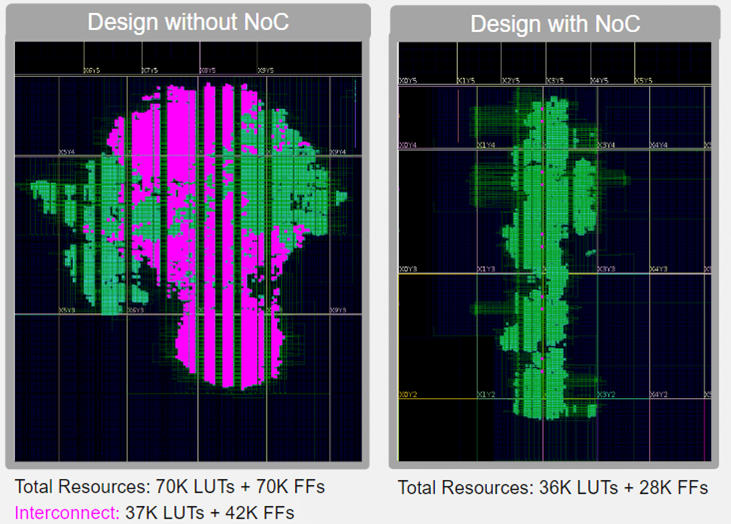
Figure 6: Resource savings through using a NoC
Intel Agilex 7 M-Series NoC
With the introduction of M-Series of Intel Agilex 7 FPGAs, NoCs are used for better memory performance. This has focused on improving access to the HBM and DDR memory interfaces of which there are many. Previously, on the Stratix-10 MX, user arbitration logic would be required if shared access between HBMs was needed. Now NoCs provide access to all HBM memories for each NAP. The Agilex M-Series device has two horizonal NoCs, top and bottom of the device, and multiple highspeed vertical NoC paths for fast access deep into the FPGA fabric. The top NoC has 20 NAPs and the bottom NoC 22 NAPs (Figure 7), which can also communicate with each other via vertical NoC paths. The number of NAPs has been designed to provide one direct connection to each attached interface, HBM, DDR and general IO groups.
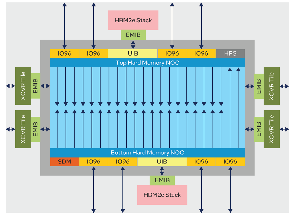
Figure 7: Agilex M-Series NoC
The Agilex 7 M-Series FPGA is featured on BittWare’s IA-860m PCIe card.
Maximizing Performance
We share some methods for optimizing connection to high-bandwidth external memory using NoCs.
The Achronix Speedster7t uses the NoC to provide access to attached GDDR6 memory. To achieve full bandwidth (56 GBytes/Sec per GDDR6, or 448 GB/s overall), each GDDR6 requires two AFUs running at least at 875 MHz, which is aggressive for the 256b-wide NAP. Given there are 8 GDDR6 memory controllers, a less aggressive application would require a minimum of 32 endpoints, running at 438 MHz with no network conflicts to saturate the GDDR6 bandwidth. Figure 8 illustrates how a 32-point endpoint design might be implemented, ensuring AFUs are distributed to avoid NoC conflicts.

Figure 8: Minimum configuration to achieve peak performance from GDDR6 memories
If AFUs require inter communication, the Speedster7t provides vertical NoC routing that can run independently of any communication happening horizontally. For the above example this would allow AFUs to exchange information without degrading memory performance over the NoC.

Figure 9: Using the vertical NoC network to communicate between AFUs
On the Agilex M-Series, the HBM memory is presented as 32 independent memory interfaces, 16 at the top and 16 at the bottom of the device. For a balanced performance the M-Series NoC has unique network routes to each memory controller, HBM and DDR, which should yield lower latency (less hops) and less conflicts on the NoC (Figure 10). The NoC also only needs to run at fabric speeds, greatly reducing power.

Figure 10: Maximizing Agilex M-Series HBM bandwidth by using multiple endpoints.
Figure 10 shows a possible configuration of a design with 32 endpoints accessing the HBM memory in parallel, with no NoC conflicts. Horizontal inter-AFU communications would need to use standard FPGA routing resources.
Saving Resources When Using High-Level Tools
FPGAs are becoming increasingly complex, with more and faster interfaces supported. The logic required to communicate to all these devices can consume a significant amount of FPGA resources. This is particularly a problem when creating high-level language board support packages (BSPs). NoCs can help here by giving the BSP easier access to as many external interfaces as possible. This allows for smaller, more flexible, and easier to develop BSPs.
Conclusion
NoCs provide a significant improvement in performance and productivity. Each chip vendor has a unique approach with different targets for the use of the NoC concept. All provide a significant step-up in performance versus not using dedicated on-chip networks—saving resources and increasing design flexibility without consuming programmable logic gates.