
White Paper
FPGA-Accelerated NVMe Storage Solutions
Using the BittWare 250 series accelerators
Overview
In recent years, the migration towards NAND flash-based storage and the introduction of Non-Volatile Memory Express® (NVMe™) have multiplied the opportunities for technology companies to “do storage” differently1. The rapid growth and diversity of real-time digital businesses has demanded this innovation to allow new products and services to be realized.
Introduction
In recent years, the migration towards NAND flash-based storage and the introduction of Non-Volatile Memory Express® (NVMe™) have multiplied the opportunities for technology companies to “do storage” differently1. The rapid growth and diversity of real-time digital businesses has demanded this innovation to allow new products and services to be realized. New storage products have therefore followed trends towards higher bandwidth, lower latency and a reduction in footprint and total cost of ownership – critical improvements for companies relying on large infrastructures. Recent market reports2 forecast that the NVMe market will grow at approximately 15% CAGR to reach $57 billion by 2020. The NVMe market continues to evolve and seeks further technological innovations in three areas:
- storage virtualization to increase flexibility and security
- localized data processing close to the stored data
- disaggregated storage for optimized infrastructures3
In March 2018, BittWare announced the 250 series FPGA products which provides innovative solutions to cater to the needs of the storage market. The 250-series product features the Xilinx® UltraScale+™ FPGAs and MPSoCs which offers ASIC-class functionality in a single-chip and fits the technology needs of the storage industry6. By combining NVMe with reconfigurable logic FPGA and MPSoC, BittWare is offering a new class of storage products with a critical differentiator in a fast-evolving market; the flexibility and reconfigurability of the Xilinx devices guarantees that 20-based solutions can remain current as the NVMe standard incorporates new features overtime5.
This application note describes how BittWare’s 250 series of FPGA and MPSoC-enabled accelerator products can be used to allow customers to construct high-performance, scalable NVMe infrastructures for next generation IoT and cloud infrastructures.
NVMe Roadmap
Since the creation of NVMe in 2011, the NVMe consortium has remained very active. In fact, the NVMe protocol is currently evolving from three perspectives defined in separate specifications. In addition to the base NVMe specification, the NVMe Management Interface (NVMe-MI) details how to manage communications and the devices (device discovery, monitoring, etc.) and the NVMe over Fabric (NVMe-oF) drives how to communicate with non-volatile storage over a network to present the protocol as transport agnostic9.
Over time, as more users from various industries start adopting NVMe, the new users characterize their need for new features and introduce new ideas for the specification. The adoption of the NVMe protocol is still growing and it is generating innovation. Hardware and software companies are finding new ways to get to the memory through the introduction of new form factors, the creation of new products and appliances, etc. The focus of the NVMe ecosystem is to give users the means to scale into the datacenter or hyperscale infrastructures, and the protocol specification will continue to evolve in that direction9.
2019 will see the release of revision 1.4 of the NVMe base specification which will lead to improvements in data latency, high-performance access to non-volatile data and ease of data sharing between several hosts. One of the features awaited by NVMe users, and cloud providers specifically, is IO determinism which will increase the quality of service during parallel execution of IOs10. By limiting the impact of background maintenance tasks to a minimum and containing the influence of noisy neighbors, the IO determinism feature will give users a consistent latency when accessing the non-volatile data. An alternative approach is the previously discussed Open Channel architecture11. With this second method, the host takes over some of the management functions and only the data travels to the storage hardware. In this configuration, the drive’s physical interface to the host is limited to high-speed data lanes, there are no sideband channels. This example shows the impact and relevance of any changes in the NVMe specification and highlights the requirements for a flexible NVMe hardware infrastructure.
As the new revisions of the base, MI and over Fabric specifications come out in the next few months, NVMe users will benefit from a flexible foundation which can adapt to the new NVMe requirements. The 250 series FPGA and MPSoC products provide this flexibility but also solve today’s customers’ challenges and give them an immediate competitive advantage.
Why FPGAs?
BittWare’s FPGA and MPSoC products feature the very latest Xilinx UltraScale+ technology and fit the need of a datacenter increasingly focused on NVMe. FPGAs have provided programmable hardware solutions to multiple industries over three decades and are broadly used to solve computing and embedded systems problems in automotive, broadcasting, medical and military markets amongst others. At the same time, in recent years, FPGA manufacturers have introduced the latest and greatest in integrated systems design improvements to this proven technology.
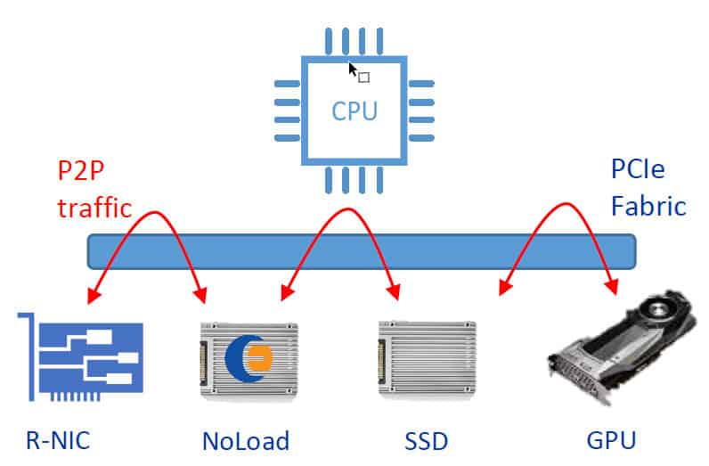
The Xilinx UltraScale+ FPGA and MPSoC products use a 16nm process and improve the system performance by providing high-speed fabric, embedded RAM, clocking, and DSP processing. Besides, Xilinx devices have introduced faster transceiver technology (up to 32.75 Gb/s) for higher throughput connectivity into the network or the PCIe fabric. With their high count of serial transceiver channels, UltraScale+ products can connect to multiple PCIe interfaces at once and provide a data offload interface to a host CPU. In some cases, by replacing a PLX switch with an FPGA or MPSoC, the CPU can offload some of its processing and free up for other operations. The programmable logic of FPGA and MPSoC also provide a deterministic and low-latency interface in a system which can give a clear competitive advantage in some use cases.
Recent FPGA families now also include embedded low-power microprocessors inside the device fabric. The UltraScale+ MPSoCs match the need of applications that require software as well as programmable logic by combining them into a single package. For example, the Xilinx Zynq UltraScale+ ZU19EG features two processing units, one Quad-core ARM Cortex-A53 and one real-time Dual-core ARM Cortex-R5, in addition to a graphics processing unit, an ARM Mali™-400 MP2, for applications with hybrid computing needs. The ZU19EG MPSoC device makes for a very versatile chip especially well-suited for NVMe over Fabric or Open Channel implementation where the programmable logic provides a low-latency deterministic path for the storage data, and the ARM cores perform complex packet control operations or replace a host CPU in a CPU-less embedded system.
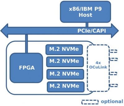
Over the last few years, BittWare has remained at the forefront of the storage industry and contributed to its innovative growth by developing products based on NVMe technology. BittWare recognized that FPGAs could reduce I/O bottlenecks and offer a direct high-speed deterministic path to NVMe solid state drives. As early as 2015, BittWare partnered with Xilinx and IBM to develop an innovative NoSQL database solution12. The 250 series FPGA & MPSoC boards builds upon the success of this initial product and adds features like deeper and faster onboard memory, network connectivity, system on chip and cabling options to server storage backplanes.
Empty heading
250 FPGA & MPSoC Product Series
The 250 FPGA & MPSoC product line comprises three FPGA adapters, the 250S+, 250-U2 and 250-SoC, which connect to a variety of industry-standard form factors like PCIe slots, OCuLink/Nano-Pitch, SlimSAS, MiniSAS HD, U.2 storage backplanes and more. The 250 series products fit right into an existing infrastructure’s PCIe fabric for direct low-latency access to the NVMe storage devices.
250S+ Directly Attached Accelerator
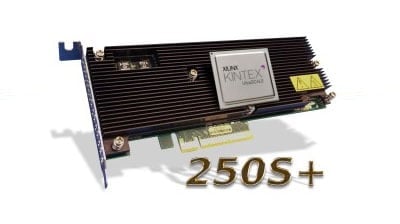
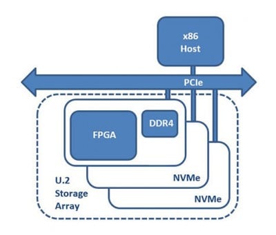
The first accelerator of the series is the 250S+. This FPGA accelerator features a Xilinx UltraScale+ Kintex 15P FPGA and four onboard four-lane 1TB M.2 NVMe drives (4TB of non-volatile flash total) in a low-profile 8-lane half-height half-length PCIe compliant form factor. Alternatively, for customers who only want to introduce FPGA computing in their system and already have storage available, the M.2 onboard connectors can cable out to OCuLink/Nano-Pitch or MiniSAS HD NVMe backplanes using Molex low-loss high-speed cabling technology. With 1,143K System Logic Cells, 1,968 DSP Slices and 70.6 Mb of embedded memory, the KU15P FPGA is the largest device of the UltraScale+ Kintex FPGA series and provides a significant amount of configurable resources to implement value-add features. The on-board DDR4 memory bank allows for additional buffering of deeper data vectors.
- Up to four M.2 NMVe SSDs coupled on-card to the Xilinx FPGA
- OCuLink break-out cabling allowing the 250S+ to be part of a massively scaled storage array
Directly Attached Accelerator (DAA)
- Virtualize the NVMe storage and share across multiple Virtual Machines
- Isolate the NVMe storage to increase security between the host CPU and the NVMe SSDs
- 250S+ & 250-SoC
250-U2 Proxy In-Line Accelerator
The second member of the 250 series is the 250-U2. This accelerator board features a Xilinx UltraScale+ Kintex 15P FPGA (same as the 250S+) and one bank of DDR4 memory in a 2.5” U.2 drive form factor. Unlike the 250S+, the 250-U2 does not have any onboard SSDs directly attached to the FPGA. The novel design of this accelerator allows it to fit into existing U.2 storage backplanes in systems with no dedicated PCIe slots for additional compute power next to existing standard U.2 NVMe storage. This 250-U2 product takes on the role of Proxy In-Line Accelerator (PIA).

The 250-U2 can perform inline compression, encryption, and hashing, but also more complex functions such as erasure coding, deduplication, string/image search or database sort/join/filter. Depending on the computing needs of an application, the backplane population would show varying ratios of 250-U2 boards for NVMe drives. The 250-U2 sits in the U.2 backplane alongside the storage and features the same maintenance options as any other standard U.2 NVMe drives leveraging the NVMe-MI specification. As both the 250-U2 processing node and the storage connect directly to the PCIe fabric of the host server, DMA data traffic can bypass the CPU and global memory entirely for optimized end-point to end-point data transfers using technology like SPDK. With RDMA or peer-to-peer DMA solutions, the data flows directly between NVMe end-point bypassing the CPU entirely. These direct interfaces into the FPGA and MPSoC programmable logic significantly reduces access latency (Lusinsky, 201721). Alternatively, another use case for this hardware platform is as an offload compute engine and would fit nicely in a FPGAaaS scalable infrastructure.
Proxy In-Line Accelerator (PIA)
- Perform low-latency, high-bandwidth processing on local NVMe storage data
- Multiple host form factors 8-lane PCIe adaptor or 2.5” U.2
- 250S+ & 250-U2
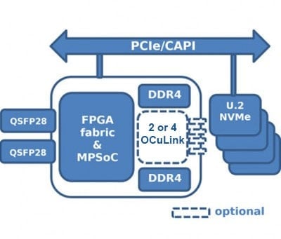
250-SoC for NVMe-over-Fabric
The third accelerator of the series, the 250-SoC, features a Xilinx UltraScale+ Zynq 19EG MPSoC and can connect to both the network fabric through two QSFP28 ports (25Gbps line rates for 100GbE support) or the PCIe fabric through a 16-lane PCIe 3.0 host interface and four 8-lane OCuLink connectors. The ZU19EG is the largest device in its series with 1,143K System Logic Cells, 1,968 DSP Slices and 70.6 Mb of embedded memory. The embedded ARM processing and graphical units in the device package creates the ideal platform for a product with hybrid processing requirements.
The 250-SoC hardware versatility allows for direct access to storage from the network and supports NVMe-over-Fabric. NVMe-oF is the next generation NVMe protocol to disaggregate storage over the network fabric and manage storage remotely; NVMe-oF also provides additional flexibility over SAS to setup a network array on demand. Disaggregated storage or EJBOF (Ethernet Just-a-Bunch-Of-Flash) hardware reduces storage cost, footprint and power in the datacenter.
The Xilinx Zynq MPSoC chip offers additional flexibility for embedded systems. The MPSoC board can run an Operating System and its full software stack independently from a host CPU. With its high-bandwidth network features supporting up to two 100GbE ports and the onboard MPSoC, the 250-SoC removes the need for both an external Network Interface Card (NIC) and an external processor for NVMe-oF applications13. The implementation of an FPGA-based NVMe-oF infrastructure is simple and performant because the data only follows through hardware paths which gives a low and predictable latency solution.
NVMe-over-Fabric (NVMEoF)
- Low-Latency and High-Throughput of NVMe frames over the datacenter network fabric
- 250-SoC
The 250-SoC provides a flexible array of solutions for the storage industry. The 250S+ and the 250-SoC tackle the need for virtualization and increased security by targeting the Direct Attached Accelerator use case. The 250-U2 and the 250S+ easily plug-in to an existing infrastructure as Proxy In-Line Accelerators to offer low-latency & high-bandwidth local data compute for the NVMe storage. And finally, the 250-SoC supports NVMe-over-Fabric as a hardware-only innovative method to disaggregate storage while supporting the latest generation NVMe protocols. As the NVMe market continues to grow, FPGAs and MPSoC solutions will solve the application challenges of NVMe products.
NVMe Applications
NVMe technology has brought disruptive innovation to storage and has a far-reaching impact on the datacenter infrastructure. The features of the protocol make NVMe the number one choice when designing a new product or application involving storage.
Enterprise applications such as database acceleration require low-latency as well as high-bandwidth 4K or 8K data write transfer rates which are two requirements that fit perfectly into the NVMe protocol strengths. These characteristics place NVMe in the lead to implement redo log, for example, a use case where many transaction records get stored and for future replay if the database fails. For this use case, the 250S+ brings up to 4TB of NVMe storage straight to the edge of the FPGA reconfigurable fabric where the transaction records get gathered to the SSDs at high-speed ready for replay14.
NVMe also alleviates the challenges of virtualized infrastructures and simplifies the implementation of VMs (Virtual Machines), stateless VMs and SRIOV where IO is the most common bottleneck. In the stateless VM use case, the IT manager needs lock down operating system images that corporate users do not modify. Users only modify their data and the OS image remains unchanged in the NVMe storage; privacy and security between users is critical. For such IT infrastructure, NVMe storage is shared between multiple users. The 250S+ is all-in-one platform to implement this application. Each 1TB physical drive gets divided by the FPGA IP so each user gets segregated and secure access to its OS image and data. The hypervisor manages the direct access to the fraction of drive without the need for an emulation driver which provides better performance for this IO bounded application.
The “Big Data” market also brings opportunities for intelligent NVMe products which combine storage and processing since it is moving away from a batching approach to a real-time processing methodology. Map reduce problems are moving towards real-time analytics instead of batching and, therefore, they need a new tier of storage which is much faster than the GFS backend. The storage tiering now seen in IT infrastructures separates cold storage rarely accessed and low speed, to very fast SSDs, NVMe or NVM memories. In this use case, all the data gets recorded in the GDFS but then it is moved to a compute node with faster memory. The 250-SoC implementing NVMe-over-Fabric answers both these requirements as it gives access to high-speed storage and high-performance compute capabilities.
The deep learning industry has similar needs to the analytics world. The new generation accelerators for deep learning, i.e., GPGPUs, TPUs and FPGAs; these devices need large memory bandwidth to match the chips’ compute abilities. The training operations consume a lot of this high-throughput data, often multiple terabytes15. Recent research efforts show that the FPGA fabric can accelerate training operations of certain network types. Therefore, combining both the storage and the compute engine onto one hardware platform reduces the latency allowing for more retraining cycles as the training dataset increases16.
In the HPC space, local storage of the 250S+ and the remote version with the 250-SoC have several applications like checkpoint/restart, burst buffer, distributed filesystems or caching the job data from a scheduler. By running the algorithm close to the storage on the FPGA fabric, the footprint of the FPGA application remains low, while utilizing the storage fully and keeping the CPU free for other processing jobs. Instead of simply storing the data or using host CPU to compress or encrypt the in-memory databases, in which gigabytes of data are held in volatile memory but need to be backed up into flash on a regular basis. An FPGA-based system can process these snapshots of data for permanent storing into large NVMe-based storage arrays. For this type of operation, the MPSoC is particularly well-suited to perform more complex operations on the user data.
Finally, in the IoT space, there is a need for data filtering and preprocessing on IoT gateways where aggregation takes place as well as encryption for data after it has been received, the FPGA processes streams of data in real-time with bit-operations like encryption or compression and stores the data away on-board using the 250S+ or passes it to the storage backplane at the input bandwidth with the cabled 250S+ or the 250-SoC. FPGAs are also the platform of choice from blockchain calculations. Blockchain technology brings a differentiation to IoT gateways to provide an adaptive and secure method to maintain user privacy preferences of IoT devices17.
BittWare’s Capabilities
For over twenty years, BittWare has helped industry specialists introduce FPGAs in their infrastructure to design, develop and optimize workloads. During that time, BittWare Compute and Network solutions have provided a competitive advantage to customers in various industries including HPC, Finance, Genomics and Embedded Computing. BittWare combines hardware, software, and system design expertise to guide customers looking to maximize the benefits of FPGA technologies in their products.
In the 250-accelerator series, BittWare has selected a variety of Xilinx UltraScale+ devices and PCIe form factors for a complete solution offering for storage infrastructure architects. These accelerators connect the programmable logic of the Xilinx devices directly into the infrastructure network, and PCIe fabric through last generation 100GbE and PCIe 3.0 high-speed interfaces. Additionally, using the capabilities of BittWare parent company Molex, the 250 series offers high flexibility to connect the existing hardware. Molex is an industry leader in ultra-high-speed low-loss cables and interconnects solutions.
Conclusion
NVMe has and is still transforming the storage industry at a rapid pace. This new high-throughput storage technology provides a flexible storage solution for IT infrastructures. NVMe not only provides superior data write and read bandwidth compared to previous generation storage, it also leverages current PCIe and network fabric of existing datacenters. As NVMe becomes more popular, industry innovators are launching new products which support NVMe. All of the basic datacenter equipment is being updated to support NVMe; NVMe storage backplanes are now the new norm.
FPGA-based products for NVMe allow the compute to merge with the storage at the hardware level to reach higher application performance. With FPGAs, the processing of reconfigurable logic is directly attached to the storage through a high-throughput and low-latency pipe. Because of these characteristics, data can flow through the FPGA and be processed in real-time. Additionally, by using FPGA processing, the CPU cores become free to perform other tasks that can only run on the processor. With MPSoCs, additional capabilities are available to the system and combine high-speed data processing and control on the device which can potentially run in autonomy.
BittWare FPGA and MPSoC-based storage products have been designed to target the needs of real applications and solve the challenges of IT infrastructure managers. BittWare offers a path to production with the 250-product series.
References
- McDowell S. (2018). Storage Industry 2018: Predictions For The Year To Come. Forbes. Retrieved June 4, 2018, from: https://www.forbes.com/sites/moorinsights/2018/01/24/storage-industry-2018-predictions-for-the-year-to-come
- Ahmad M. (2017). Four trends to watch in NVMe-based storage designs. Electronic Designs. Retrieved June 8, 2018, from: https://www.electronicproducts.com/Computer_Peripherals/Storage/Four_trends_to_watch_in_NVMe_based_storage_designs.aspx
- G2M Research (2018). G2M Research NVMe Ecosystem Market Sizing Report. G2M Research. Retrieved June 6, 2018, from: http://g2minc.com/g2m-research-nvme-ecosystem-market-sizing-report
- Mehta N. (2015). Pushing Performance and Integration with the UltraScale+ Portfolio. Xilinx. Retrieved June 8, 2018, from: https://www.xilinx.com/support/documentation/white_papers/wp471-ultrascale-plus-perf.pdf
- Allen D., & Metz J. (2018a). The Evolution and Future of NVMe. Bright Talk. Retrieved from: https://www.brighttalk.com/webcast/12367/290529
- Nuncic (2017). More Speed for your SSD – NVME Expected to Replace SATA and SAS in the Future. OnTrack. Retrieved June 8, 2018, from: https://www.ontrack.com/blog/2017/09/15/nvme-replace-sata-sas/
- Adshead A. (2017). Storage briefing: NVMe vs SATA and SAS. Computer Weekly. Retrieved June 8, 2018, from: https://www.computerweekly.com/feature/Storage-briefing-NVMe-vs-SATA-and-SAS
- Rollins D. (2017). The Business Case for NVMe PCIe SSDs. Micron website. Retrieved from: https://www.micron.com/about/blogs/2017/july/the-business-case-for-nvme-pcie-ssds
- Allen D., & Metz J. (2018b). On the Horizon for NVMe Technology: Q&A on the Evolution and Future of NVMe Webcast. NVM Express. Retrieved from: https://nvmexpress.org/on-the-horizon-for-nvme-technology-qa-on-the-evolution-and-future-of-nvme-webcast/
- MaharanP. (2018). A Review of NVMe Optional Features for Cloud SSD Customization. Seagate Blog. Retrieved from: https://blog.seagate.com/intelligent/a-review-of-nvme-optional-features-for-cloud-ssd-customization/
- Martin B. (2017). I/O Determinism and Its Impact on Datacenters and Hyperscale Applications. Flash Memory Summit 2017. Retrieved from: https://www.flashmemorysummit.com/English/Collaterals/Proceedings/2017/20170808_FB11_Martin.pdf
- Leibso S. (2016). IBM and Nallatech demo CAPI Flash at OpenPOWER Summit in San Jose. Xcell Daily Blog. Retrieved June 4, 2018, from: https://forums.xilinx.com/t5/Xcell-Daily-Blog/IBM-and-Nallatech-demo-CAPI-Flash-at-OpenPOWER-Summit-in-San/ba-p/691256
- SakalleyD. (2017). Using FPGAs to accelerate NVMe-oF based Storage Networks. Flash Memory Summit. Retrieved June 7, 2018, from: https://www.flashmemorysummit.com/English/Collaterals/Proceedings/2017/20170810_FW32_Sakalley.pdf
- Rollins J. D. (n.d.). Redo Log Files and Backups. Wake Forest University. Retrieved from: http://users.wfu.edu/rollins/oracle/archive.html
- Wahl M., Hartl D., Lee W., Zhu X., Menezes E., & Tok W. H. (2018). How to Use FPGAs for Deep Learning Inference to Perform Land Cover Mapping on Terabytes of Aerial Images. Microsoft Blog.
- Teich D. (2018). Management AI: GPU and FPGA, Why They Are Important for Artificial Intelligence. Forbes. Retrieved from: https://www.forbes.com/sites/davidteich/2018/06/15/management-ai-gpu-and-fpga-why-they-are-important-for-artificial-intelligence/#6bf2ff171599
- Cha S. C., Chen J. F., Su C., & Yeh K. H. (2018). Blockchain Connected Gateway for BLE-Based Devices in the Internet of Things. IEEE Access. Retrieved from: https://ieeexplore.ieee.org/document/8274964/
- Alcorn (2017). Hot Chips 2017: We’ll See PCIe 4.0 This Year, PCIe 5.0 In 2019. Tom’s Hardware. Retrieved June 8, 2018, from: https://www.tomshardware.com/news/pcie-4.0-5.0-pci-sig-specfication,35325.html
- Caulfield L. (2018). Project Denali to define flexible SSDs for cloud-scale applications. Azure Microsoft. Retrieved June 6, 2018, from: https://azure.microsoft.com/en-us/blog/project-denali-to-define-flexible-ssds-for-cloud-scale-applications/
- Ismail N. (2017). Flash storage: transforming the storage industry. Information Age. Retrieved June 4, 2018, from: http://www.information-age.com/flash-storage-transforming-storage-industry-123465174/
- Lusinsky R. (2017). 11 Myths about RDMA over Converged Ethernet (RoCE). Electronic Design. Retrieved June 9, 2018, from: http://www.electronicdesign.com/industrial-automation/11-myths-about-rdma-over-converged-ethernet-roce
- Miller R. (2017). IBM’s new Power9 chip was built for AI and machine learning. Tech Crunch. Retrieved June 8, 2018, from: https://techcrunch.com/2017/12/05/ibms-new-power9-chip-architected-for-ai-and-machine-learning/
- Peng V. (2015). 16nm UltraScale+ Series by Victor Peng, EVP & GM. Xilinx. Retrieved June 8, 2018, from: https://www.xilinx.com/video/fpga/16nm-ultrascale-plus-series.html
- Vaid K. (2018). Microsoft creates industry standards for datacenter hardware storage and security. Azure Blog. Retrieved from: https://azure.microsoft.com/en-us/blog/microsoft-creates-industry-standards-for-datacenter-hardware-storage-and-security/
- Retrieved from: https://blogs.technet.microsoft.com/machinelearning/2018/05/29/how-to-use-fpgas-for-deep-learning-inference-to-perform-land-cover-mapping-on-terabytes-of-aerial-images/