
White Paper
Building NVMe Over Fabrics with BittWare FPGA Solutions
Overview
Since the introduction of the Non-Volatile Memory Express (or NVMe) protocol, data center customers have broadly adopted this new technology, which brings higher performance and low latency to storage applications (Gupta, 2018). The feature set of NVMe has made the technology the fastest-growing storage solution in the market. By 2021, International Data Corporation predicts that NVMe-based storage solutions will be generating more than 50% of the revenues associated with primary external storage shipments (Burgener, 2019).
BittWare provides FPGA acceleration solutions to implement basic hardware offloads (compression, de-duplication, etc.) plus application-specific algorithms such as machine learning applications using FPGAs for inference. This mix of basic and advanced acceleration of storage at performance levels matching NVMe is what we call computational storage. Our 250 series of products, including the 250S+, 250-SoC, and 250-U2, focus on this market.
Recently the NVMe consortium introduced a variant of the protocol called NVMe over Fabrics (NVMe-oF), to leverage the benefits of NVMe over existing network infrastructures. As data centers continue to see an expansion of on-premise NVMe storage, remote users can access disaggregated storage with little overhead using NVMe-oF (Gibb, 2018). This requires implementing a specialized network stack in hardware to maintain the NVMe advantages of low latency and high bandwidth.
Our solution uses an FPGA with on-chip ARM processor, the Xilinx Zynq MPSoC on our 250-SoC board. The FPGA acts as the NVMe-oF controller, offloading from the CPU or even decoupled from the CPU when using the on-chip processor. We deliver low latency and high bandwidth by fully implementing the NVMe data plane in FGPA logic, including the network protocol stack. The ARM core is in the design to handle the control plane using software where latency and bandwidth are less of an issue. This Application Note describes how to configure the BittWare 250-SoC as an NVMe-oF controller in a JBOF.
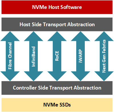
What is NVMe Over Fabrics
The NVMe-oF protocol uses the high-speed SSD technology and expands it beyond a local server or data center.
NVMe-oF allows the application developer to access remote storage nodes on network fabrics such as Fiber Channel, InfiniBand, RDMA (Remote Direct Memory Access) over Converged Ethernet (RoCE), iWARP and more recently TCP/IP while keeping latency low (typically between 10us for a cluster of a 100 NVMe drives to 100 additional microseconds for large clusters). In short, an NVMe-oF transaction involves a host and a target; the target is the server exposing the NVMe block storage devices across the network for the host server to access (Davis, 2018). With RDMAs, the host-target data transfers can occur without the CPU handling the transaction; instead, dedicated RNICs pass the data between resources with a low impact on computing resources as the part of the hardware in the NIC manages the transport layer of the network stack.
Why use FPGA for NVMe-oF?
You basically have three choices when you decide to offload NVMe-OF into a PCIe card:
First, you can use an ASIC implementation, which would be the lowest cost and lowest latency choice. However ASICs don’t allow you to also offload “computational storage” algorithms. ASICs are also generally only available for the most popular network bandwidths, which are rarely the highest bandwidths.
Second, you could use a system-on-a-chip with a high core count, which would allow you to add “computational storage” algorithms. However, doing so requires parallel programming skills. The ultimate solution is generally the highest latency of the choices here which works directly against NVMe’s low-latency value proposition. Like ASICs, these MPP SOCs are generally only available for the most popular network bandwidths which are rarely the highest bandwidths.
Third, you can use an FPGA. This option allows you to add “computational storage” algorithms while maintaining ASIC-like latency. This option also enables high-bandwidth networks such as 100 or even 400Gb. Although it may be the most expensive of the three options, the cost difference becomes only slightly higher when you consider the volumes involved in storage markets.
Adaptive Storage
By leveraging technologies like FPGAs and SoCs, datacenter architects can further reduce data movement to/from the CPU for data-intensive operations. With hardware-driven acceleration, user applications show higher performance and lower response times. As the number of free CPU cycles increases, the processes distributing workloads take advantage of the hybrid system architecture using dedicated hardware and the CPU more efficiently. The FPGA fabric architecture, their IO throughput, and their programming flexibility facilitate the design of reconfigurable hardware tightly coupled with high-bandwidth NVMe storage. FPGAs are particularly suitable for compression, encryption, RAID and erasure code, data deduplication, key-value offload, database query offload, video processing, or NVMe virtualization, for example. FPGA hardware offers the performance of a dedicated solution but also has the advantage of being reconfigurable quickly switching purpose as the datacenter needs change over time.
Using a Xilinx MPSoC for NVMe-oF Target
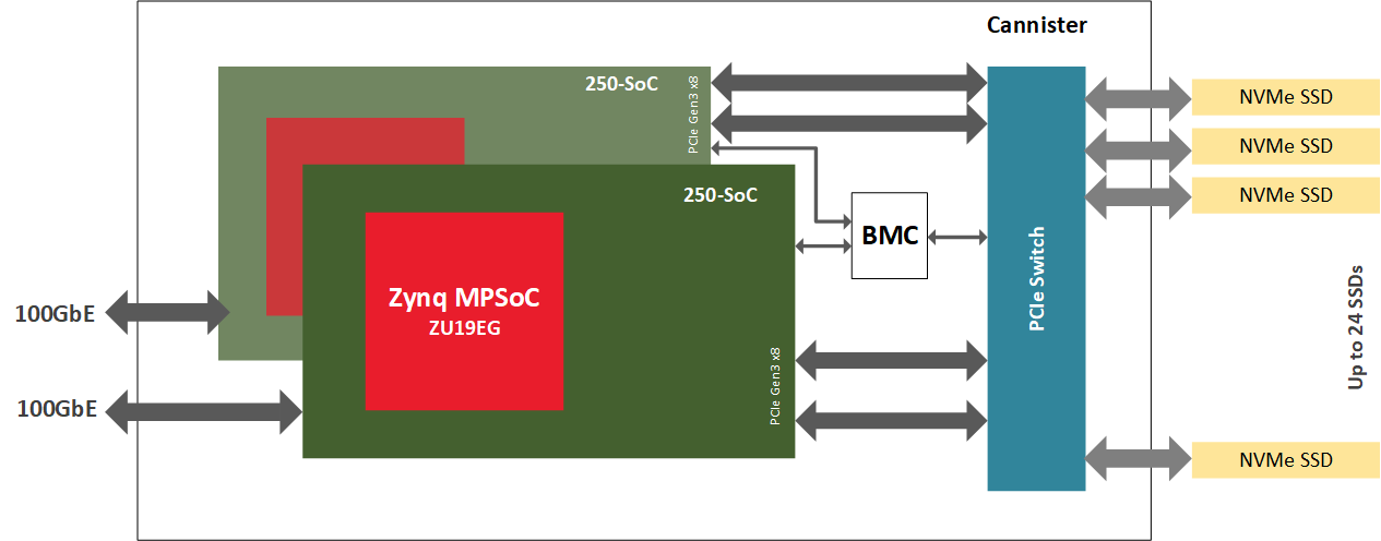
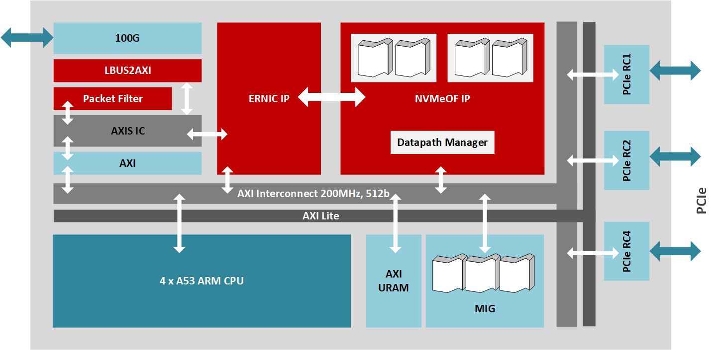
The BittWare 250-SoC features a Xilinx UltraScale+ Zynq ZU19EG MPSoC and can connect to both the network fabric through two QSFP28 ports and the PCIe fabric through a 16-lane host interface or four 8-lane OCuLink connectors. This MPSoC adaptor is a perfect platform to drive an NVMe-oF target node as it combines data stream compute in the FPGA fabric (also called, PL, or Programmable Logic), network IO, PCIe connectivity, and an onboard ARM processor. Note that the ARM is not in the data plane; it handles control plane work. Placing a dedicated hardware accelerator between the CPU and storage endpoints creates a system optimized to compute closer to the data.
The Hardware
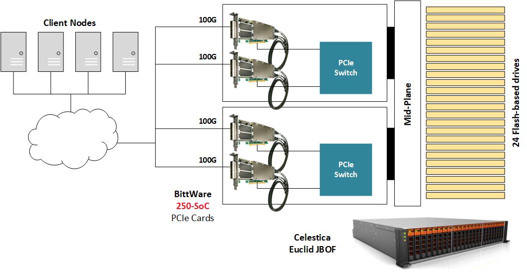
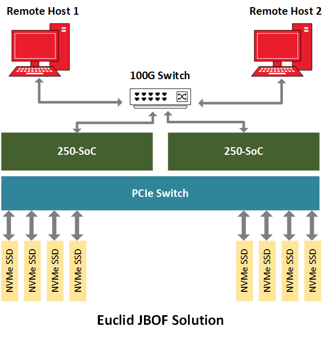
To demonstrate NVMe-oF, BittWare places the 250-SoC inside a JBOF (Just-A-Bunch-Of-Flash) chassis populated with several NVMe U.2 drives and exposes the QSFP28 ports of the 250-SoC board to the network. The Celestica Euclid JBOF features two plug-in blades with a PCIe switch and a PCIe slot; each drawer acts as the conduit between the network fabric and the NVMe storage. The NVMe packets transit from the QSFP28 ports to the FPGA fabric, and then they go through the PCIe host interface, the JBOF’s PCIe switch, before finally reaching the NVMe drives. In this implementation, the 250-SoC OCuLink connectors are not in use, but in a different hardware platform, they could accommodate a cabled version of this design where PCIe transactions would run over cables.
The Gateware
The design implements an NVMe-oF target for RoCE v2 (NVMe 1.2 and NVMe-oF 1.0 spec compliant) which supports explicit congestion management. The IP targeting the MPSoC uses several of Xilinx IP library blocks all interconnected through a 512-bit AXI bus running at 200MHz for the data plane. The Xilinx Embedded RDMA NIC processes the 100Gb/s network traffic, while a PCIe root complex IP core manages the connectivity to the 16-lane PCIe 3.0 interface to the JBOF circuitry driving up to 24 drives, and a DMA core controls the high-speed data transfers over the AXI bus. Additionally, the NVMe-oF target core manages up to 256 queues over the 100Gb/s data path while firmware running on the quad-core A53 ARM processor handles high-level administration of the storage node.
Maximizing Performance
The MPSoC PL can accommodate the maximum bandwidth of the data path. Therefore, to demonstrate the maximum capabilities of the overall system, the host must generate network traffic as close to 100Gb/s as possible. For benchmarking, a couple of NVMe-oF hosts connect to a network switch which then can feed the maximum data throughput to the 250-SoC MPSoC card running the NVMe-oF target in the JBOF. This reference design shows around 2.5 MIOPS random read performance and over 1.1M random write performance while showing an application latency of 105 us.
Advantages of Reconfigurable Hardware Solutions
An MPSoC-based NVMe-oF solution presents several advantages compared to a software (CPU + external NIC + SPDK) or an RNIC solution (CPU + integrated NIC). If an MPSoC-based solution has a relatively high cost and power consumption compared to other products, such technology outperforms the competition from a bandwidth, configurability, and latency perspective. Similarly, to an RNIC solution, the MPSoC NVMe-oF will saturate the network interface throughput. However, the MPSoC hardware implementation offers levels of flexibility and adaptability that other solutions do not have. This adaptive hardware can, therefore, target domain-specific applications allowing system architects to combine customer defined features (RAID, or new NVMe features as the spec evolves) with the primary IP and enhance the overall system feature set. Another option is to add custom accelerators like encryption or compression, for example, to combine two functions in one box. Finally, solution providers can create application-specific hardware products optimized for a specific purpose like video processing (video codec, for example) or artificial intelligence workloads. By combining an IT function like storage management with a task typically performed by an expensive compute node, the CPU gets relieved from having to perform high-bandwidth IO transfers and gets repurposed to more compute critical operations. From a latency perspective, the MPSoC-based solution provides a low and predictable latency over CPU-driven alternatives.
Conclusion
As NVMe matured over the last few years, it has paved the way for NVMe-oF, which now offers similar benefits to NVMe to disaggregated storage environments (Weaver, 2019). The technology has improved compute and storage nodes utilization while increasing agility and performance in the data center (Waever, 2019). NVMe-oF allows developers to target applications in novel ways, for example, AI workloads which require random reads over vast datasets (several 100s PB) will significantly benefit from this technology (Hemsoth, 2019). FPGA and MPSoC provide an extra layer of innovation on top of the NVMe-oF protocol; the programmable logic in these devices allows the design of system architecture that can handle high bandwidth data transfers, low latency while also remaining configurable for optimizations or application-specific customization. BittWare offers a range of NVMe acceleration options including for NVMe-oF — get in touch with us to learn more.
References
- Burgener E. (2019). Three Providers of High-Performance Storage Interconnect NVMe over TCP Named IDC Innovators. AP News. Retrieved May 6th, 2019, from APNews.com
- Gibb S. (2018). FPGA Accelerator Disaggregation Using NVMe-over-Fabrics. SNIA. Retrieved July 1st, 2019, from SNIA.org
- Gupta R. (2018). What is NVMe™, and why is it important? A Technical Guide. Western Digital Blog. Retrieved June 24th, 2019, from Blog.WesternDigital.com
- Hemsoth N. (2019). Existing Storage Infrastructure is the Bottleneck for AI. Next Platform. Retrieved May 6th, 2019, from NextPlatform.com
- Robinson D. (2019). VAST Data guarantees no downtime, no data loss. Blocks & Files. Retrieved May 6th, 2019, from BlocksAndFiles.com
- Rouse M. (2019). Computational Storage. Tech Target. Retrieved June 24th, 2019, from SearchStorage.TechTarget.com
- Weaver E. (2019). Top 5 Reasons M&E Needs NVMe Now. Media & Entertainment Service Alliance. Retrieved May 6th, 2019, from mesalliance.org