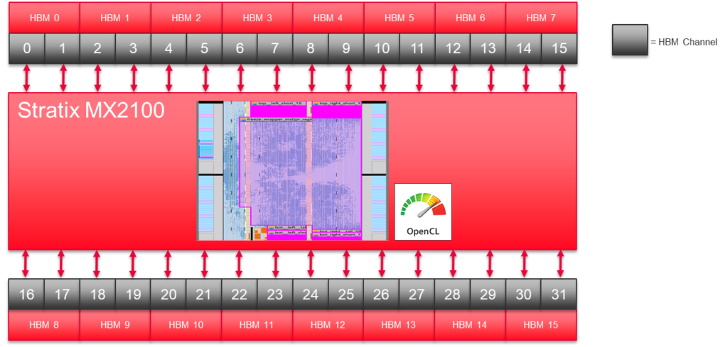
 The Stratix 10 MX has 32 pseudo HBM2 memory channels. Our 2D FFT implementation uses half those channels.
- We can place two 2D FFT kernels in the chip. One kernel uses all the pseudo channel interfaces on the north side of the chip. The other uses the channels on the south side.
- Trying to use all 32 channels in a single 2D FFT creates routing challenges we did not want to deal with in demonstration code.
One Row per FPGA HBM2 Channel
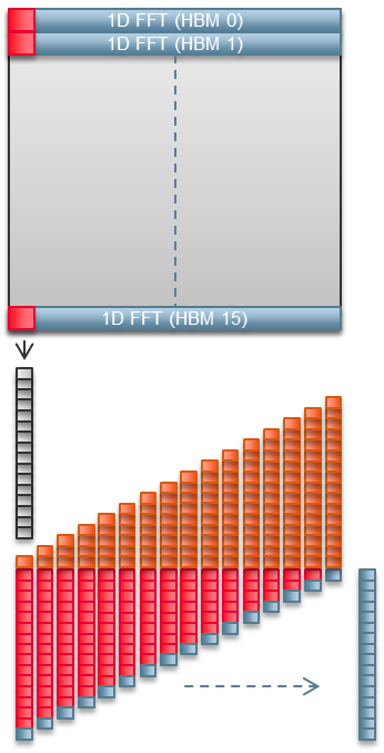
The 2D FFT is implemented using many 1D FFTs. A single 1D FFT saturates the HBM2 channel it uses. With 16 HBM2 channels, our 2D FFT implementation processes 16 rows of the 1024 row matrix in parallel. A high-end GPU can probably process all 1024 rows in a single pass. The FPGA requires 64 passes. However, number of passes does not matter as HBM2/GDDR6 bandwidth is the limiting factor in both cases.400 MHz Fmax is Enough
We need a 400 MHz OpenCL clock frequency to saturate each HBM2 channel doing the optimal 32-byte bursts. Going faster has no value. Going slower is not optimal. Intel’s current implementation of DPC++ leverages BittWare’s existing OpenCL board support package. Thus both implementations look like OpenCL to the FPGA. Both implementation require the same tweaks to achieve 400 MHz. These tweaks are just expressed differently in source code.1D FFT Output
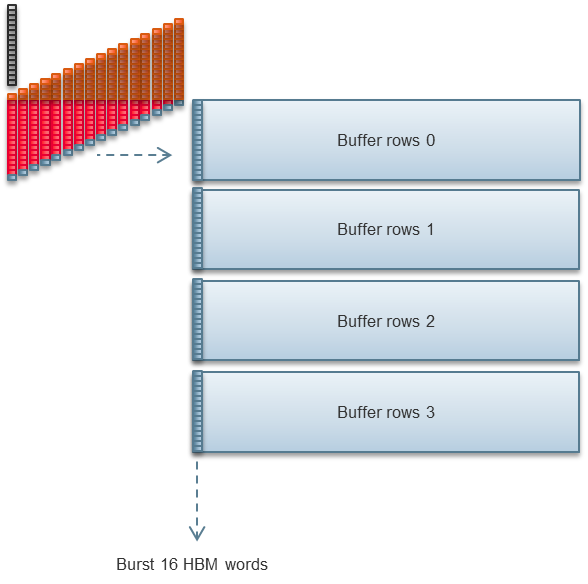
The 1D FFT does not output results directly into HBM2. Instead it writes into FPGA internal memory. Additional FPGA logic collects the results of multiple 1D FFTs, corner turns those results, and writes them back to HBM2, all in parallel with computation.