
White Paper
Comparing FPGA RTL to HLS C/C++ using a Networking Example
Overview
Most FPGA programmers believe that high-level tools always emit larger bitstreams as the “cost” for the higher productivity. But is this always true? In this paper we show a real-world example where we created a common network function, RSS, using both traditional RTL/Verilog tools and then using high-level synthesis (HLS) on the same hardware. What we found was surprising: the HLS approach actually used fewer FPGA gates and memory. There is a reason. Read on for details.
The HLS approach to FPGA development is to only abstract portions of the application that can be easily expressed in a C/C++ environment. The HLS tool flow is available for essentially any BittWare board through the use of Vivado (Xilinx) or Intel (Quartus) tools.
To succeed with HLS, it’s important to recognize the portions of your application that will be a good fit. Guidelines include:
- Target uses are, generally, IP blocks that are defined in a high-level language to begin with. A math algorithm would work well or, as in our RSS block, some network protocol processing.
- Another category of uses are blocks that are poorly defined and thus may require multiple rounds of implementation. The biggest benefit here is allowing the HLS tool to automatically pipeline the resulting native FPGA code, often emitting fewer stages than quickly hand-coding a pipeline will. Also, when it comes time to modify the hand-coded pipeline, delay changes on one parallel path can have a ripple effect on everything. Using the HLS tool to automatically pipeline a second time, from scratch, eliminates that headache.
- Finally, an HLS flow makes it easier to port code between FPGA brands and speed grades. This is because HLS automatically generates the appropriate number of pipeline stages—something you need to manually specify when working with Verilog or VHDL.
The current limitations of HLS are clearly that its scope is limited to IP blocks. The application team would still require RTL for other components, although leveraging something like BittWare’s SmartNIC Shell for the RTL parts, a user may be able to define their unique application entirely in HLS. It should also be noted that HLS is a poor choice for the most simplistic of codes or larger designs that consist mostly of pre-optimized components.
Our Application: Networking RSS on an FPGA
What is RSS? RSS stands for “Receiver Side Scaling.” It is a hashing algorithm to efficiently distribute network packets across multiple CPUs. RSS is a feature on modern Ethernet cards, and generally implements the specific Toeplitz hash defined by Microsoft.
The environment that hosts our RSS application is BittWare’s SmartNIC Shell. The SmartNIC Shell is designed to give users head start when building an FPGA-based networking application. It provides users an optimized FPGA-based 100G Ethernet pipeline, including DPDK for host interaction. All the user needs to do is drop in their application as an IP block.
In this case, BittWare was the user as well, having created as our application an FPGA implementation of RSS. The team creating RSS using the traditional RTL approach and the HLS team both were able to use SmartNIC Shell as their FPGA Ethernet framework and concentrate on the RSS application itself.
BittWare’s RSS Implementation
Our FPGA-based RSS implementation is specifically based on C code found in the DPDK source tree, with the test function for that code also available in the tree. Our RSS application also uses a 64-entry indirection table instead of the more common 128-entry table. What is important for this HLS study is that the function we are moving into the FPGA starts off defined in C. That meets our number one criterion for HLS success—a definition in C or C++.
Grouping Packets Using Tuples
The goal of the the RSS function is to distribute packets among CPUs, keeping related streams of packets together. Different Toeplitz key sets provide different distribution patterns. However, no matter the key set, our RSS function uses each packet’s source and destination IP address and source and destination ports as input. These four components combined are called a 4-tuple.
Note that for our RSS application we are assuming the 4-tuple was already parsed and added to the packet’s metadata. Another SmartNIC Shell module handles this packet classification function. We call that module our “parser” and will be the subject of a separate BittWare white paper.
Our RSS implementation currently accepts a 96-bit field for classification—enough for the 4-tuple of IPv4 source/destination and port. The parser provides zero for fields not available in the packet; if a packet does not include any IP payload, the full 96-bit tuple field is zero.
Many RSS implementations use a 5-tuple instead of a 4-tuple. Doing that would require an additional 8-bits to accommodate the protocol number. HLS users of RSS can easily accommodate that change with minor source code changes. This ability to quickly adapt from 4-tuple to 5-tuple is an example of the number two criteria for HLS success – a requirement for multiple rounds of implementation.
FPGA Development Tool Terms
Developing IP to run inside an FPGA traditionally uses languages originally created for ASIC development. There isn’t consensus regarding what to call these languages. Sometimes people use “RTL” which stands for register transfer language. Other people use “HDL” which stands for hardware definition language. The two most popular HDLs are VHDL and SystemVerilog. Internally BittWare uses both but our larger projects use SystemVerilog and it full verification feature set.
Verification is an important part of the FPGA design process and is a critical part of ASIC design. Rising costs in the ASIC industry drove the need for advanced verification languages and techniques to ensure first pass silicon success. This need drove the Verilog language to incorporate features of HVLs (High level Verification Languages), eventually merging into the current SystemVerilog IEEE 1800 standard. Modern ASIC verification has also moved toward a Universal Verification Methodology (UVM) that provides a standard way of building testbenches.
The different economics of FPGA development as well as the ability to immediately test designs in the lab have slowed the adoption of UVM among FPGA developers. Nevertheless, the growing complexity of high-density FPGAs has pushed many groups to adopt the same verification methodology that is used in ASIC design flows. At BittWare, we have a fluid approach to FPGA verification. We often use simple testbenches based on the SystemVerilog or VHDL features available in inexpensive or free simulators. When appropriate, however, we build modern testbenches based on the full feature set of SystemVerilog and UVM.
HLS, or High Level Synthesis, is the name given to languages which operate at a higher level of abstraction than HDL. In practice, HLS usually refers to specialized versions of C or C++. However, there are other HLS languages. For example, some third-party IP that BittWare distributes is written in BlueSpec. All of these HLS tools tend to come with an easy, push-button way to generate a testbench at the module-level. UVM is still needed at the system level.
Finally, at the highest level today, is OpenCL. It is a parallel programming language developed for GPU chips and repurposed into the FPGA world. Today OpenCL’s application is almost entirely HPC, or high-performance computing, where it is used to implement computational algorithms that run faster than an Intel-based server can run them.
HLS Coding for Performance
Although using HLS provides a software-like tool flow, the developer must still learn hardware-centric concepts, such as pipelining and iteration intervals, that they may have not been exposed to in writing C-code for traditional processors.
HLS code is predominately used to develop IP components for embedded designs, usually pipelined. Our RSS application is no exception. For RSS, the minimal performance requirement is that each 512-bit input word is processed fast enough to keep up with a saturated 100 Gb/s network interface. This equates to a new word processed every clock cycle at a frequency of 300MHz. This frequency is challenging in that even the fastest FPGAs run at frequencies not much higher than 400MHz. Clearly, we must process a new word every clock.
This introduces the concept of Iteration Interval (II) which refers to the number clock cycles required for a given piece of logic in a pipeline to complete. For the RSS module we required a result every clock, an II of 1. Therefore, we need to understand how to write code that avoids breaking this requirement.
Causes of higher II include the following:
- Inter loop dependencies are caused when the next output of a pipeline requires the future result of another variable in a pipeline, e.g. recursion. Simple recursive operators such as accumulators are permitted as FPGA’s contain logic to accomplish these calculations within a single clock cycle. However, more complicated recursion will require higher II values.
- The RSS design requires that each stage of the pipeline completes within 3.3ns. The HLS tools will insert registering where required to ensure each stage meets this timing requirement. However, it’s not always possible to do so if the combinatorial logic cannot be pipelined. Examples of are deep combinatorial logic can be indexing calculations for multiple nested loops.
- The II will increase if the target clock frequency is too high and the FPGA fabric routing paths are simply too long to meet the timing requirement. A solution to this problem would be to split logic into two paths running at half the clock frequency.
The main body of the code loops over the number of required input tuple words creating a new hash. For the example here we use an input tuple of 3 words for a hash value of 96 bits.
					int input_len = 3;

/*
* The hash calculation is calculated per input tuple word.
*/
int32_t ret = 0;
int j, i;
for (j = 0; j < input_len; j++) {
    for (i = 0; i < 32; i++) {
        if (tuple_in_i[j] & (l << (32 - i ))) {
            ret ^= rte_cpu_to_be_32(((const uint32_t *)rss_key) [j]) << i |
            (uint32_t) ((uint64_t) (rte_cpu_to_be_32 (((const uint32_t *)rss_key) [j + 1])) >>
            (32 - i));
        }
    }
}
return ret;
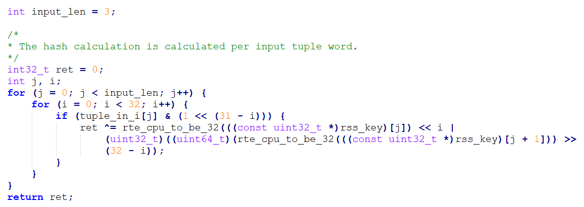
This code implements the heart of the RSS calculation. It remains unchanged from the original extracted from the DPDK source tree. Thus, in the case of this RSS block, all of the porting work was in defining the block’s AXI interfaces and adding pragma statements to definings like II.
If the input length is a constant the FPGA can completely unroll the two loops to create fully pipelined code.
To integrate the IP component into the Smart NIC frame work the interfaces and control plane need to be defined, along with any logic to read and write to external interfaces. The smart NIC framework uses the AXI interface protocol to communicate between components.
Defining AXI interfaces and adding pragma statements resulted in too many lines of code to show in a figure here. The full source code file is available from BittWare.
There is an endianness challenge as the Xilinx compiler’s constants are in Intel byte order (little-endian) but networking protocols use network byte order (big-endian). This does not affect performance or resource use but requires that any input data has its endianness changed before it is processed in HLS.
Native Programming Versus HLS: The Results
The reason we have two FPGA RSS implementations is because our initial version was written in Verilog. This happened under the assumption we are evaluating: that native FPGA coding always results in the smallest resource usage. However, a BittWare engineer challenged that decision and reimplemented RSS in HLS to test this approach. He was right and BittWare has now replaced the RSS module and the Parser module in our SmartNIC Shell with HLS code.
Two RSS Implementations
| Characteristic | Verilog | HLS C |
|---|---|---|
| CLBs | 44,435 | 2,385 |
| BRAM | 12 | 1 |
| Registers | 52,352 | 4,843 |
| Lines of Code | 650 | 459 |
The biggest difference between the two implementations is that the Verilog/RTL version uses FIFOs and the HLS C++ version does not. We were surprised to see resource usage actually went down by moving to HLS—something we would not expect in all cases.
What about the time savings? Roughly speaking, we saw a timeline of a month for the native RTL version, while the HLS code was completed in a week.
Intel HLS versus Xilinx HLS
This example uses Xilinx HLS. However, one key advantage of using high level languages is their ability to abstract, to certain extent, the underlying differences between different technology architectures. Intel also have an equivalent compiler which also compiles C++ to gates RTL code.
In order to compile the same code using the Intel i++ compiler, some subtle changes to data types and changes to #pragmas are required. The biggest difference between Intel and Xilinx is the use of Avalon streaming interfaces for Intel and AXI for Xilinx. This would require a simple shim interface to convert from one to the other.
Co-Simulation
Once functionally is verified it is a trivial task to invoke the co-simulation environment for cycle accurate RTL simulation. Vivado-HLS automatically generates an RTL testbench which is driven by vectors generated by the original C++ code. The only modification required by the user is to handle any infinite loops or blocking interfaces in their design. The RSS module is designed to run indefinitely as part of a firmware pipeline. Therefore, the simulation would never complete and the co-simulation would hang. To avoid this, we change the “while (1)” main loop of the RSS code to be a fixed length long enough to consume all inputs from the testbench and long enough to generate all the outputs required.
Co-simulation gives an extra level of confidence that the RTL has been generated correctly by the tool and timing characteristics of the module fit within the original design parameters.
The co-simulation flow is also available as part of the Intel HLS tool stack.
HLS Building by IP Blocks
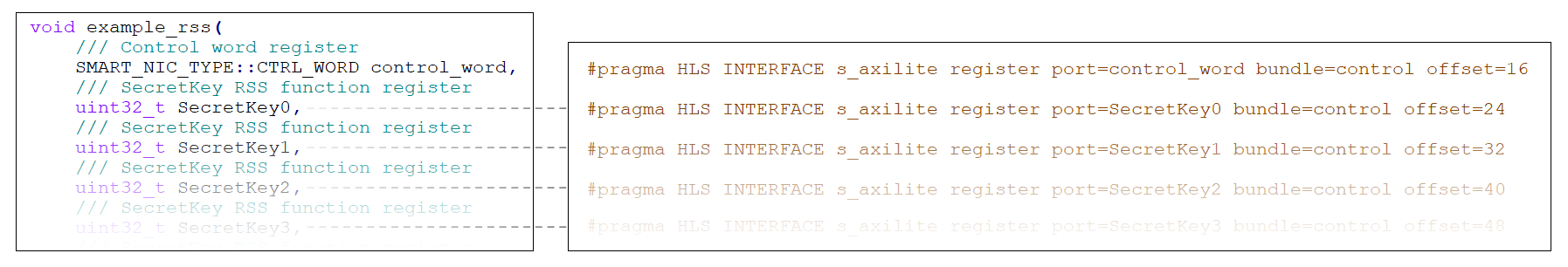
The HLS tool flow needs to have built-in awareness of the interface protocols used. IP blocks from BittWare generally use Advanced extensible Interface (AXI) to communicate. Specifically, an AXI4-Stream to pass packet data and AXI4-Lite as a control plane.
For 100 GbE, BittWare uses an AXI4-Stream interface that is 512 bits wide and clocked at 300 MHz. The metadata associated with each packet follows on its own bus that is valid at the end of a packet, when the packet data’s TLAST signal is asserted. The packet metadata evolves between blocks and between releases. It usually includes information about:
- The number of the physical Ethernet connector that the packet arrived on
- Any errors the MAC identified associated with the packet
- A timestamp in 80-bit IEEE-1588 format or sometimes in a shortened 64-bit format
- A “deleted” bit to indicate the packet needs to be removed from the stream at the next opportunity
- A number we usually call “queue” to indicate a destination for the packet. It is calculated by one of the IP blocks in the pipeline (maybe even this block)
Our control plane for the RSS block includes:
- An enable/disable bit
- Twenty 16-bit keys for the Toeplitz hash
- A 64-entry indirection table
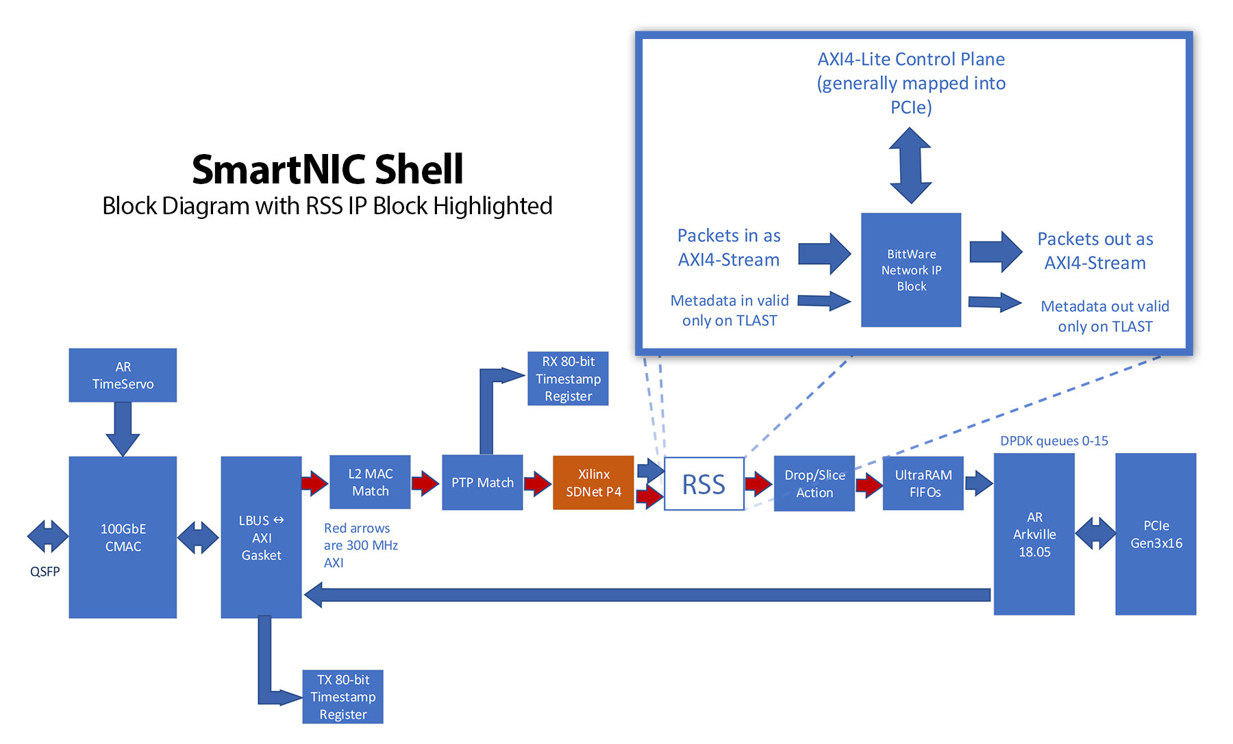
SmartNIC Shell block diagram of example implementation of the SmartNIC Shell framework. Here the RSS block is replaced with an HLS implementation.
Conclusion
Today’s high-level FPGA development tools are designed to reduce time-to-market and reliance on hardware engineers. However, the assumption that use of these tools always brings a compromise in application performance—either in speed or silicon resources—is false.
We found using HLS to develop IP blocks for BittWare’s SmartNIC Shell cut the development time from about a month to one week. We also found it actually used fewer gates to implement.
The source code for the RSS block is available for XUP-P3R board owners and users of the SmartNIC Shell. It’s an excellent illustration of how to use AXI interfaces within HLS code. Contact a BittWare representative to learn more.
HLS, in addition to native development tools, is available for all BittWare FPGA boards. We also offer a range of boards supporting OpenCL development—click here to learn more.