Satellite dish

White Paper

PCIe Data Capture

Overview

High-resolution sensors can generate data rates that require FPGA pre-processing to reduce their output to something that a host computer can capture and process. If the post-FPGA data rate exceeds about 40 Gb/sec, moving that data into the host requires specialized solutions.

BittWare has architectural concepts that are flexible for the needs of the customer’s IP and reduce cost.

This white paper covers the Data Capture component of BittWare’s High-Speed Data Capture and Recorder concepts. We explain some of the techniques used to achieve sustained 100 Gb/s capture into host DDR4 over a PCIe bus.

Architectural Goal for PCIe Data Capture

This concept’s goal is achieving 100 Gb/s out of the FPGA and into a motherboard where customers can process that data using many CPU cores. It moves data from the FPGA card over PCIe and the CPU to the host DDR4. There are optional components to record to persistent memory (requiring a dedicated CPU for this task) and adding a second PCIe for capturing 200 Gb/s to DDR4 using two CPUs.

The Data Capture concept is available on the BittWare Developer website for customers with AMD and Intel FPGA-based products. It consumes 12% of the AMD Virtex UltraScale+ VU9P FPGA. Adapting the project to another BittWare Agilex or UltraScale+ card is relatively easy for customers to do themselves. 

Data capture illustration
App note thumbnails
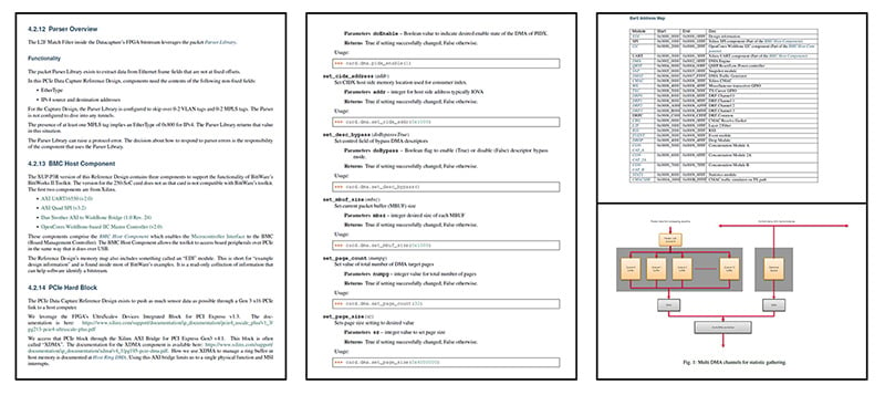
Sample pages from the Data Capture App Note

Request the App Note

Need even more details than this white paper provides? Request the App Note, which gives the documentation for our Data Capture concept. Click here >>

How We Achieved 100 Gb/s PCIe Data Capture

PCIe Theory vs. Practice

Theoretically PCIe Gen 3 can transfer 985 MB/s per lane. For 16x that means 15.760 GB/s (126 Gb/s) in each direction—well over our 100 Gb/s goal. However, there are layers of protocol as well as buffer management along the path. An excellent academic paper that explores this is Understanding PCIe performance for end host networking by Rolf Neugebauer.

In practice, BittWare’s PCIe Data Capture was able to push 12.8 GB/s (102 Gb/s) from the FPGA into host DRAM. That is just over 80% of PCIe’s theoretical maximum transfer speed.

The reality for PCIe transfer in practice is much lower and is heavily influenced on the particular approach used to optimize the system. Achieving 100 Gb/s is actually a good way of stressing PCIe—for very large packet sizes, 100 Gb Ethernet (GbE) approaches 12.5 GB/s, leaving 300 MB/s headroom for metadata. However, when a saturated 100 GbE consists of all tiny packets, the overall data rate is much lower, but the number of PCIe bus transactions can go up, stressing PCIe in a different way.

We use Ethernet to stand in for the proprietary sensors that BittWare customers commonly use. Our solution can pass both large packets and tiny packets without dropping any. Next, we will explain how we did it.

Implementation Part 1: Optimizing the Host

When pushing high bandwidth data through PCIe, one optimization is actually not inside the FPGA, but on the host’s software side. Look at the CPU’s internal architecture.

In order to achieve our performance goal, every CPU core that sits between the chip’s PCIe interface and the DRAM interface must run at full clock speed (no power-saving mode), even if that core is doing no other work. Put another way, each CPU core needs to be in C-State zero and P-State zero. In Linux, one way to achieve this is using the “tuned-adm” command and picking its “latency-performance” option.

CPU architecture illustration

Implementation Part 2: Optimizing PCIe

Optimizing PCIe Transactions Through Consolidation

The most important thing on the FPGA side is to minimize the number of PCIe transactions required to move the data over the bus. This means consolidating multiple packets in a buffer management scheme designed to allow every PCIe transaction to achieve the system’s negotiated “Maximum Payload” size, generally 256 bytes in modern, Intel-based systems.

So, a primary function of BittWare’s offering is to perform this consolidation function. We consolidate the packets into a fixed-size buffer that we call an MBUF.

The MBUF size can be changed at FPGA initialization. As we stated, the MBUF needs to be a fixed multiple of the PCIe maximum payload size. We recommend using 4k byes for a reason discussed later.

It is very common in FPGA processing to group packets for processing by separate threads of control. We call these groupings “queues” and each queue needs to flow to a different processing core on the host side. Thus, packet consolidation needs to happen on a per-queue basis.

Our consolidation function is written in HLS and it runs above a queue management function we discuss next.

Packet concatenation illustration

Host Queues

Our IP sends its stream of MBUFs into host DRAM. Like everyone else who does this, we use circular queues in DRAM. However, on AMD, we don’t use their QDMA queues, instead creating our own alternative above QDMA’s bridging function.

The AMD QDMA queues are based upon RDMA data structures. RDMA is a more dynamic environment than we need. Our version has descriptor rings, but our host driver loads the descriptors at FPGA initialization time and we reuse them. Doing it this way avoids sending descriptors over PCIe at runtime. In addition, as an even bigger deviation, we do not have completion queues. Instead we just reuse descriptors and let the host software figure out if the FPGA is moving data faster than the host can process that data. Put another way, instead of dropping data in the FPGA, we drop data on the host. In RDMA terms, the host driver never sends CIDX updates into the FPGA.

Our queue implementation uses polling on the host side instead of interrupts. This is because interrupts consume more PCIe bandwidth as the FPGA needs to send PIDX updates to the host in both approaches. Experimentation has shown that, with a modern CPU, PIDX updates need to happen after transferring a sequence of MBUFs totaling 4k bytes. That is why we recommend just making a single MBUF 4k bytes.

Over on the host side, we allow our queue descriptors to point at huge pages. Doing this minimizes CPU TLB misses. We can also allocate our huge pages in specific host NUMA zones, depending upon the location of the FPGA card, to control the route through for FPGA DMA transfers relative to host processing threads, which are also locked to particular NUMA regions.

The first release of Data Capture is layered above AMD XDMA. The second release will transition to our own DMA transport layered above AMD QDMA’s bridging mode.

Host Control

Our PCIe Data Capture concept uses the standard Linux VFIO driver. This enables the CPU’s virtualization hardware to provide process protection and security. We provide a Python API to control the card(s). We use a Python program to load the descriptors into the FPGA, setup the DRAM queues, and kickoff the application code. BittWare’s Toolkit currently does not support VFIO as a driver but support is planned for the future.

Application Processing

BittWare’s processing framework on the host side is modelled after DPDK (Data Plane Development Kit). We use a single target queue on the host. A dedicated core parses the incoming MBUFs, sending MBUF pointers off to a collection of worker threads. A dedicated core can do this task at any MBUF size.

We plan to release sample worker programs that reformat our internal data structures into PCAPng format. Reformatting requires about four worker cores to keep up with line rate 100 GbE for any packet size.

Additional Options for PCIe Data Capture Architectural Concept

There are two optional components of the concept, one adds a Recording element to SSD and the other uses the XUP-P3R’s ability to have a second PCIe interface to allow up to 200 Gb/s capture.

100 Gb/s Record

With a two-socket motherboard, it is possible to record a 100 GbE packet stream. The BittWare IP captures the packets into host DRAM attached to one of the sockets.  Application software then moves the MBUFs over the QPI links between processor sockets, into RAID 0 NVMe attached to the PCIe on the other CPU socket. A future White Paper will explain how this is done. In summary, many more NVMe drives are required than you might think. It is because NVme drive datasheets for the popular TLC SSDs tend to specify the write performance into their Pseudo-SLC caches. Overflow that cache and write performance drastically drops off. The very newest QLC SSDs can actually be slower than old fashioned disk technology on long, endless, streaming writes!

200 Gb/s Over Dual PCIe

By adding a 3rd slot add-on card in a TeraBox with two CPUs, the XUP-P3R can achieve 200 Gb/s over two Gen3 x16 PCIe interfaces!

Dual PCIe Data Capture

For customers requiring more than 100 Gb/s capture, another option is to utilize the XUP-P3R’s SEP to PCIe add-on card. This can achieve up to approximately 200 Gb/s to host memory. The second connection goes in an adjacent PCIe slot. Note that this option will consume a second CPU, without the option to also record at line rate to persistent memory.

Customers could also just use two FPGA cards on a motherboard with two or more CPUs.

Illustration of XUP-P3R with expansion card connected to dual CPUs

Conclusion

Sensors today are getting faster which leads to two CPU challenges. First with getting the I/O into the CPU and second getting the sensor data transformed into actionable information. FPGAs are often used to close this gap with hardware pre-processing, however even the reduced data volume is enough to still stress the CPU in many cases.

In this white paper, we investigated how to maximize the PCIe bandwidth to capture up to 100 Gb/s, including using the CPU—capturing to DRAM. That still leaves the potential for stressing the CPU, and so in the next white paper we will bypass the CPU entirely for recording direct to NVMe.

BittWare is using its years of experience helping customers squeeze data into a CPU to generate architectural concepts to solve these problems. Armed with these, and the ability to deploy at scale by leveraging BittWare’s broad portfolio of FPGA cards and integrated servers, customers can readily construct data capture and recorder appliances for specific use cases. Follow BittWare’s social media channels to stay up to date on the latest publications.

There's More to Read: Get the Data Capture App Note

Request PDF Download

What you see on this page is the introduction to BittWare’s Data Capture. There’s a lot more detail in the full App Note! Fill in the form to request access to a PDF version of the full App Note.

App note thumbnails
Sample pages from the Data Capture App Note

"*" indicates required fields

Name*
Please check this is an active email as the PDF will be sent using this address.
Address and City*